
When I first joined Raspberry Pi as a software engineer four and a half years ago, I didn’t know anything about chip design. I thought it was magic. This blog post looks at the journey to Raspberry Silicon and the design process of RP2040.
RP2040 has been in development since summer 2017. Chips are extremely complicated to design. In particular, the first chip you design requires you to design several fundamental components, which you can then reuse on future chips. The engineering effort was also diverted at some points in the project (for example to focus on the Raspberry Pi 4 launch).
Once the chip architecture is specified, the next stage of the project is the design and implementation, where hardware is described using a hardware description language such as Verilog. Verilog has been around since 1984 and, along with VHDL, has been used to design most chips in existence today. So what does Verilog look like, and how does it compare to writing software?
Suppose we have a C program that implements two wrapping counters:
void count_forever(void) { uint8_t i = 0; uint8_t j = 0; while (1) { i += 1; j += 1; }
}
This C program will execute sequentially line by line, and the processor won’t be able to do anything else (unless it is interrupted) while running this code. Let’s compare this with a Verilog implementation of the same counter:
module counter ( input wire clk, input wire rst_n, output reg [7:0] i, output reg [7:0] j
); always @ (posedge clk or negedge rst_n) begin if (~rst_n) begin // Counter is in reset so hold counter at 0 i <= 8’d0; j <= 8’d0; end else begin i <= i + 8’d1; j <= j + 8’d1; end
end endmodule
Verilog statements are executed in parallel on every clock cycle, so both i and j are updated at exactly the same time, whereas the C program increments i first, followed by j. Expanding on this idea, you can think of a chip as thousands of small Verilog modules like this, all executing in parallel.
A chip designer has several tools available to them to test the design. Testing/verification is the most important part of a chip design project: if a feature hasn’t been tested, then it probably doesn’t work. Two methods of testing used on RP2040 are simulators and FPGAs.
A simulator lets you simulate the entire chip design, and also some additional components. In RP2040’s case, we simulated RP2040 and an external flash chip, allowing us to run code from SPI flash in the simulator. That is the beauty of hardware design: you can design some hardware, then write some C code to test it, and then watch it all run cycle by cycle in the simulator.

The downside to simulators is that they are very slow. It can take several hours to simulate just one second of a chip. Simulation time can be reduced by testing blocks of hardware in isolation from the rest of the chip, but even then it is still slow. This is where FPGAs come in…
FPGAs (Field Programmable Gate Arrays) are chips that have reconfigurable logic, and can emulate the digital parts of a chip, allowing most of the logic in the chip to be tested.
FPGAs can’t emulate the analogue parts of a design, such as the resistors that are built into RP2040’s USB PHY. However, this can be approximated by using external hardware to provide analogue functionality. FPGAs often can’t run a design at full speed. In RP2040’s case, the FPGA was able to run at 48MHz (compared to 133MHz for the fully fledged chip). This is still fast enough to test everything we wanted and also develop software on.
FPGAs also have debug logic built into them. This allows the hardware designer to probe signals in the FPGA, and view them in a waveform viewer similar to the simulator above, although visibility is limited compared to the simulator.


The RP2040 bootrom was developed on FPGA, allowing us to test the USB boot mode, as well executing code from SPI flash. In the image above, the SD card slot on the FPGA is wired up to SPI flash using an SD card-shaped flash board designed by Luke Wren.

In parallel to Verilog development, the implementation team is busy making sure that the Verilog we write can actually be made into a real chip. Synthesis takes a Verilog description of the chip and converts the logic described into logic cells defined by your library choice. RP2040 is manufactured by TSMC, and we used their standard cell library.

Chip manufacturing isn’t perfect. So design for test (DFT) logic is inserted, allowing the logic in RP2040 to be tested during production to make sure there are no manufacturing defects (short or open circuit connections, for example). Chips that fail this production test are thrown away (this is a tiny percentage – the yield for RP2040 is particularly high due to the small die size).
After synthesis, the resulting netlist goes through a layout phase where the standard cells are physically placed and interconnect wires are routed. This is a synchronous design so clock trees are inserted, and timing is checked and fixed to make sure the design meets the clock speeds that we want. Once several design rules are checked, the layout can be exported to GDSII format, suitable for export to TSMC for manufacture.

(In reality, the process of synthesis, layout, and DFT insertion is extremely complicated and takes several months to get right, so the description here is just a highly abbreviated overview of the entire process.)
Once silicon wafers are manufactured at TSMC they need to be put into a package. After that, the first chips are sent to Pi Towers for bring-up!

A bring-up board typically has a socket (in the centre) so you can test several chips in a single board. It also separates each power supply on the chip, so you can limit the current on first power-up to check there are no shorts. You don’t want the magic smoke to escape!

Once the initial bring-up was done, RP2040 was put through its paces in the lab. Characterising behaviour, seeing how it performs at temperature and voltage extremes.

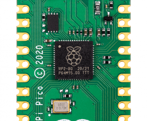
Once the initial batch of RP2040s are signed off we give the signal for mass production, ready for them to be put onto Pico boards that you have in your hands today.

A chip is useless without detailed documentation. While RP2040 was making its way to mass production, we spent several months writing the SDK and excellent documentation you have available to you today.
Website: LINK
Schreibe einen Kommentar
Du musst angemeldet sein, um einen Kommentar abzugeben.